A milestone for the global semiconductor industry was reached as the world’s first engineering validation line for 2D semiconductor technology went operational in Chuansha Town, Pudong New Area, Shanghai. The facility, developed by a consortium of Chinese tech firms and research institutions, is positioned as a cornerstone of China’s ambition to “overtake on a new track” in advanced chip manufacturing – an arena long dominated by U.S., South Korean, and Taiwanese players.
2D semiconductors, distinguished by their atomic-scale thickness (often just a few nanometers) and near-zero leakage electrical properties, represent a paradigm shift from traditional silicon-based chips. For decades, chip miniaturization relied on “carving” ever-smaller features into silicon wafers – a process now nearing physical limits at the 2nm node. 2D materials, by contrast, allow manufacturers to stack ultra-thin layers like “building blocks”, turning chip production into a “puzzle assembly” that bypasses many of silicon’s constraints.
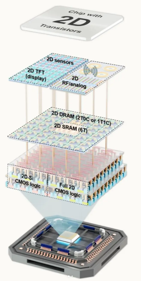
Industry analysts say the Shanghai validation line is critical to translating lab-scale 2D research into industrial viability. The facility will test production processes, material stability, and yield rates for 2D-based chips, with a focus on advancing toward 1nm process nodes – a threshold that current silicon technology may never reach. If successful, the line could enable China to achieve a “Chinese-style overtaking” in advanced chip manufacturing, breaking through the bottlenecks of foreign technology restrictions that have constrained its access to cutting-edge silicon fabrication tools.
“For years, China’s chip industry has been playing catch-up in silicon.” Said Dr. Li Wei, a semiconductor researcher at Tsinghua University. “2D materials give us a parallel track – one where we can compete at the front from the start. This validation line isn’t just a factory; it’s a bet on redefining the future of chips.”
The launch comes amid intensifying global competition in next-generation semiconductor technologies. U.S. and European firms have also invested heavily in 2D material research, but China’s move to operationalize a validation line puts it ahead in the race to industrialize the technology. The facility is expected to attract partnerships with domestic chip designers and equipment makers, creating a localized ecosystem for 2D semiconductor supply chains – reducing reliance on imported tools and materials.
Local government officials in Pudong noted that the validation line is part of a broader $15 billion regional initiative to build a 2D semiconductor industrial cluster by 2030, encompassing R&D centers, pilot production lines, and talent training programs. “This isn’t just a single project.” Said a Pudong economic development official. “It’s the start of a new chapter for China’s high-tech manufacturing – one where we lead, not follow.”
While challenges remain – including scaling 2D material production to mass-market yields and ensuring compatibility with existing chip design workflows – the launch signals China’s determination to reshape the global semiconductor hierarchy. For now, the Shanghai line stands as a tangible symbol of the industry’s shifting tides: from silicon’s “carving era” to 2D’s “assembly age”.