A research team co-led by Politecnico di Milano in Italy has developed a new “smart” chip with an innovative architecture. The chip can significantly cut energy use while ramping up data processing speed. It is expected to break the long-standing bottleneck of computing energy consumption.
The relevant findings were published in Nature Electronics on January 14th, 2026. This research marks a key step toward developing more compact, efficient and sustainable computing devices. It holds broad application prospects across multiple fields, including artificial intelligence (AI), large-scale data processing, next-generation wireless communications, robotics, data centers and 5G/6G networks.

The chip is built on a memory computing architecture. Its core advantage lies in addressing the problem of frequent data transfer between memory and processors in traditional computing systems. By reducing internal data movement, it achieves higher energy efficiency and faster processing speeds. The team demonstrated a fully integrated analog accelerator, manufactured using standard Complementary Metal-Oxide-Semiconductor (CMOS) technology, which can solve both linear and nonlinear equations.
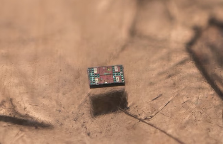
The chip integrates two 64×64 programmable resistive memory arrays. Each array arranges memory cells in a grid pattern. The cells are based on static random-access memory (SRAM) technology and incorporate integrated resistors to achieve multi-level programmable resistance. In addition, the chip integrates analog processing components, including operational amplifiers and analog-to-digital converters, forming an innovative analog computing architecture.

This design allows complex computing tasks to be completed directly within the memory structure. There is no need to transfer data to external processors, thus drastically reducing computing latency. Practical tests show that the chip delivers lower power consumption, shorter computing time and smaller chip area, while maintaining accuracy levels close to those of traditional digital systems.
The research team stated that this integrated chip proves the industrial feasibility of innovative architectures such as analog computing. The team is now working to advance the application of this technology in real-world scenarios, especially in the AI field, to reduce energy consumption during computing processes.
This work represents the outcome of international cooperation between academia and industry. Participating institutions include universities and research teams from multiple countries, all working together to promote the development of analog in-memory computing for high-performance and high-energy-efficiency applications.
